Semiconductor Manufacturing Material Solutions: Wafer Processing, Wet Benches, & FM 4910 Cleanroom Systems
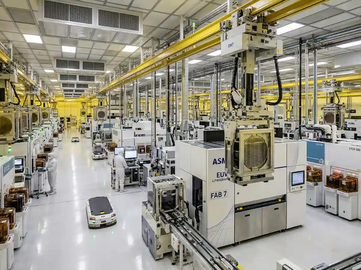 Interstate Plastics supplies high-performance, semiconductor-grade plastics engineered for extreme chemical resistance, high purity, and strict cleanroom compliance. We support equipment manufacturers and wet bench fabricators with materials that maintain dimensional stability and prevent contamination in the most aggressive fab environments.
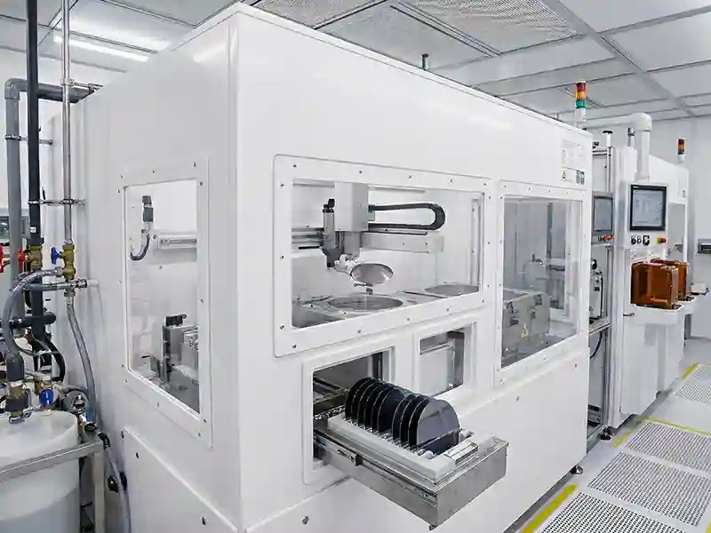
Beyond standard sheets and rods, we specialize in cut-to-size shapes, CNC-machined components, and fabrication-ready assemblies. By delivering reliable, repeatable parts, from PVC FM 4910 workstation structures to high-purity PEEK wafer nests, we help you reduce in-house rework, improve build consistency, and keep your production systems online. Featured semiconductor materials include:
- FM 4910 PVC: Flame-retardant cleanroom structures and wafer processing enclosures
- PFA / PTFE: Ultra-high purity fluid handling, chemical-resistant liners, seals, and fittings
- PVDF: Ozone-resistant tanks and high-purity fluid handling systems
- PEEK: ESD-safe wafer handling, anti-static CMP components, and low-outgassing vacuum parts
Key Materials for Semiconductor Manufacturing
Interstate Plastics supplies materials for wafer processing, chemical etching, wet benches, and cleanroom fabrication, including:
- PVC FM 4910:
- Fire-compliant workstation cabinets, wafer processing enclosures, and cleanroom structures
- Polypropylene (including FM-rated grades):
- Corrosion-resistant wet benches, chemical tanks, rinse stations, and secondary containment systems
- PVDF (Kynar®):
- Ozone-resistant chemical tanks, high-purity fluid handling systems, and oxidative wet process equipment
- PFA / PTFE:
- Ultra-high purity fluid handling, PFA tubing for ozonated UPW, chemical-resistant liners, seals, and fittings
- ECTFE (Halar®):
- High-purity tanks and liners with superior resistance to aggressive acids and chemical permeation
- PCTFE (Kel-F®):
- High-purity, low-permeability components for specialized cryogenic or high-pressure gas environments
- CPVC:
- High-temperature chemical processing systems, piping, and structural components
- PEEK:
- Precision machined components, CMP retainer rings, wafer nests, and low-outgassing parts for vacuum etching
- Polycarbonate:
- High-impact machine guards, protective enclosures, and static-dissipative cleanroom panels
- Acrylic:
- High-clarity inspection windows, cleanroom partitions, and visibility components designed to minimize particle cling
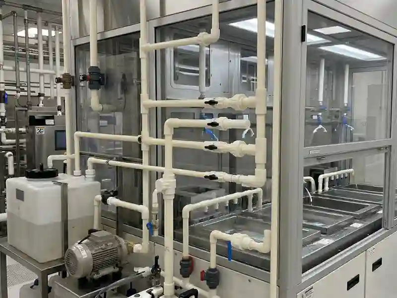
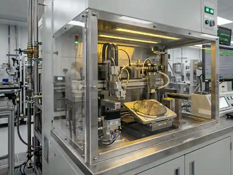
PVC FM 4910 for Workstations and Cleanroom Structures
 PVC FM 4910 is a go-to choice for semiconductor manufacturing environments that require both fire compliance and chemical resistance. It is commonly used for workstation cabinets, wafer processing enclosures, and cleanroom structures where exposure to acids, solvents, and ultra-pure water is routine.
Unlike general-purpose plastics, PVC FM 4910 is engineered to meet strict fire performance standards while maintaining structural integrity and resistance to chemical attack. Its ease of fabrication, including welding and machining, makes it well suited for building complex workstation systems and enclosures used throughout wafer processing and wet bench operations.
For semiconductor equipment manufacturers and fabricators, PVC FM 4910 helps address challenges such as fire risk in cleanrooms, material degradation in chemical environments, and inconsistent performance across builds. By sourcing pre-qualified, compliant materials, manufacturers can standardize workstation designs, reduce downtime from material failure, and maintain reliable performance across high-demand semiconductor production systems.
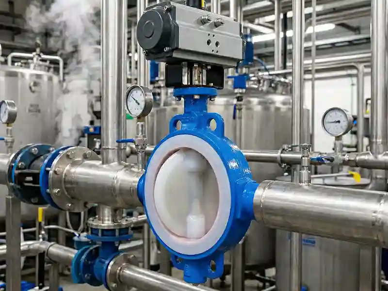
Polypropylene for Wet Benches, Tanks, and Chemical Processing
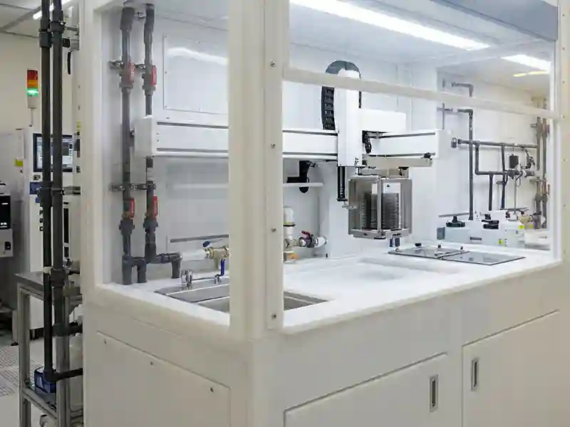 Polypropylene is a reliable material for semiconductor wet bench fabrication, chemical tanks, and rinse systems where chemical resistance and cost efficiency are key. It performs well in environments exposed to acids, bases, and cleaning solutions, making it a reliable option for wet processing applications. Compared to higher-end materials, polypropylene offers a strong balance of durability, lightweight handling, and ease of fabrication, which makes it ideal for large tanks, structural components, and general-purpose chemical handling systems.
Across semiconductor fabrication environments, polypropylene helps reduce corrosion, simplify welding and assembly, and lower overall system costs. It is commonly used in rinse tanks, secondary containment, and wet bench structures where extreme purity or high-temperature resistance is not required. This improves build efficiency, reduces material waste, and supports consistent performance across processing systems.
PVDF (Kynar®) for Chemical Handling and Wet Process Equipment
 PVDF (Kynar®) is frequently selected for semiconductor wet processing, chemical etching equipment, and fluid handling systems that require high purity and long-term durability. It provides excellent resistance to strong acids, solvents, and ozonated ultrapure water (UPW) while maintaining mechanical strength and dimensional stability under demanding conditions. Because PVDF is highly resistant to oxidative degradation caused by ozone, which is a common agent in wafer cleaning cycles, it is a preferred material for ensuring the structural integrity of high-cycle process vessels.
In semiconductor environments, PVDF helps mitigate issues such as premature material failure, contamination risk, and inconsistent performance in harsh chemical conditions. It is widely used in chemical tanks, process vessels, and fluid delivery systems where reliability is essential. This helps extend equipment life, improve consistency across builds, and maintain stable wafer processing conditions even in highly oxidative environments.
ECTFE (Halar®) for High-Purity Chemical Resistance
 ECTFE (Halar®) is commonly used in semiconductor wet bench systems and chemical processing equipment that require high-purity performance and superior corrosion resistance. It performs reliably in highly aggressive chemical environments, including strong acids and oxidizers, while maintaining low permeability and long-term durability. Compared to standard plastics, ECTFE is better suited for applications where preventing chemical attack and maintaining material integrity are critical.
When used in semiconductor processing systems, ECTFE helps address challenges such as chemical permeation, material degradation, and shortened service life in demanding environments. It is commonly specified for tanks, liners, and fluid handling components where chemical integrity and contamination control are essential.
PCTFE (Kel-F®) for High-Purity Gas Handling and Cryogenic Applications
 PCTFE (Kel-F®) is a go-to material for semiconductor and gas handling applications that require extremely low permeability and high purity in demanding environments. It performs reliably in cryogenic and high-pressure gas systems where maintaining barrier integrity is critical, making it well suited for seals, valve components, and specialized containment parts.
Compared to other plastics, PCTFE offers superior resistance to gas diffusion while maintaining excellent dimensional stability, allowing it to be integrated into precision-engineered systems.
In semiconductor and advanced processing applications, PCTFE helps address challenges related to gas leakage, contamination, and performance consistency under extreme conditions. It is often used in high-purity and cryogenic environments where material reliability directly impacts system safety and efficiency.
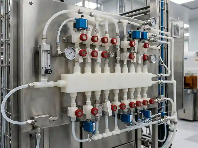
PFA and PTFE for Ultra-High Purity Fluid Handling
 PFA and PTFE are the gold standards for semiconductor fluid handling, chemical etching systems, and ultrapure water (UPW) delivery. These plastics are chemically inert, providing near-universal resistance to aggressive acids and solvents while ensuring extremely low extractables and leachables.
PFA (Perfluoroalkoxy) is the preferred choice for the highest-purity "wet-end" applications because it is melt-processible, resulting in smoother internal surfaces that prevent particle entrapment and bacterial growth. Furthermore, both PFA and PTFE offer superior ozone resistance, making them the only reliable options for fluid lines exposed to the high-purity ozonated water used for advanced wafer sanitization.
In modern fab environments, PFA and PTFE are critical for maintaining the parts-per-trillion (ppt) purity levels required for advanced nodes. They help prevent contamination that could otherwise lead to wafer defects and reduced yield.
CPVC for Chemical Processing Systems
 CPVC is a go-to material for semiconductor chemical processing systems that require improved temperature resistance and stronger chemical compatibility than standard PVC. It performs reliably in wet bench environments exposed to elevated temperatures and corrosive chemicals, making it well suited for piping systems, tanks, and structural components. CPVC provides a higher performance threshold than standard PVC while still maintaining ease of fabrication, allowing it to be integrated into complex semiconductor equipment designs.
In semiconductor applications, CPVC helps overcome limitations associated with standard PVC, particularly in higher-temperature or more aggressive chemical environments. It is often used as a cost-effective upgrade for chemical processing equipment where moderate performance improvements are needed. This helps improve system durability, reduce material failure, and maintain consistent performance.
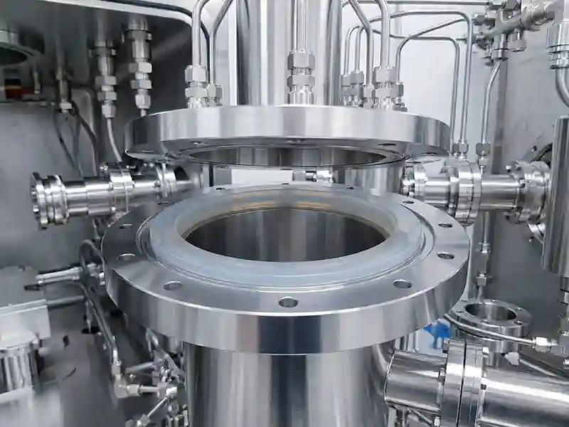
PEEK for Precision Components, Etching, and CMP Applications
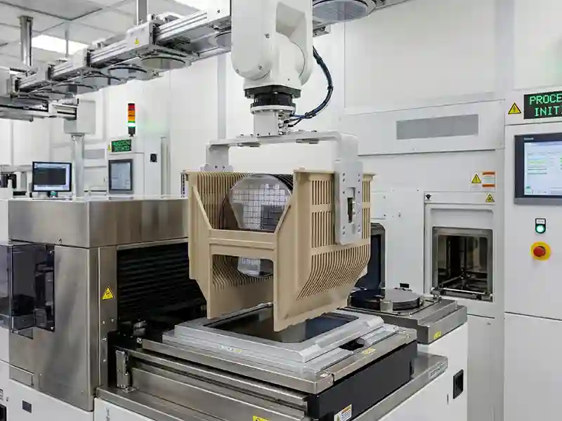 PEEK (Polyetheretherketone) is a high-performance thermoplastic used in semiconductor manufacturing for precision machined components, including wafer carriers, nests, and CMP (Chemical Mechanical Planarization) retainer rings. It offers exceptional mechanical strength, wear resistance, and dimensional stability, allowing it to maintain tight tolerances and survive high-cycle mechanical stress. PEEK’s low-outgassing characteristics make it ideal for high-vacuum etching environments, while its ability to withstand elevated temperatures ensures reliability in advanced 3D stacking and thermal processing.
For semiconductor equipment manufacturers, PEEK addresses critical challenges such as material deformation under load and premature wear in abrasive slurry environments. Beyond standard grades, ESD-safe (Electrostatic Dissipative) PEEK prevents sudden static discharge that can damage sensitive sub-5nm nodes. Our machinable PEEK shapes support the production of high-durability substrates, insulators, and wear parts that directly improve process yield and extend the service life of consumable tool parts.
Polycarbonate for Machine Guards and Protective Enclosures
 Polycarbonate is a high-performance material used in semiconductor manufacturing for machine guards, protective enclosures, and cleanroom panels that require extreme impact resistance. It offers unmatched toughness and long-term durability, making it ideal for environments where operator safety and equipment protection are paramount. Polycarbonate maintains excellent optical clarity, providing a secure barrier against physical impact and debris without obstructing the view of critical processes.
In modern semiconductor equipment design, specialized ESD-safe (electrostatic dissipative) polycarbonate is often required to prevent the buildup of static charges that can attract airborne contaminants or cause discharge events near sensitive wafers. Polycarbonate, including static-control and FM-approved grades, helps manufacturers balance safety, visibility, and ESD compliance. By using materials engineered to reduce static attraction, equipment builders can improve part consistency and streamline the integration of protective panels into advanced wafer processing systems.
Acrylic for Inspection Windows and Cleanroom Visibility
 Acrylic a trusted material for semiconductor applications requiring maximum optical clarity, such as inspection windows, cleanroom partitions, and high-resolution visibility components. It provides a polished, distortion-free surface with superior light transmission, allowing for precise monitoring of automated processes with minimal visual interference. Compared to other transparent plastics, acrylic delivers a more refined aesthetic finish and high UV resistance, which is essential for maintaining clarity in controlled environments over long service cycles.
In enclosed semiconductor systems, acrylic enhances usability by allowing operators to conduct clear visual audits of internal wet processing and handling operations. It is commonly utilized in workstation panels and enclosures where high-definition visibility is the primary requirement. Acrylic, including anti-static coated options that minimize particle cling, helps ensure inspection windows remain clear and clean.
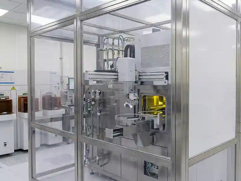
Custom Cut Panels, Machined Components, and Fabricated Parts for Semiconductor Equipment
Custom-cut panels and fabricated plastic components help semiconductor equipment manufacturers, wet bench fabricators, and fluid handling system builders standardize critical parts and reduce variability across production systems. Wet bench panels, chemical tanks, process enclosures, workstation cabinets, ducting components, wafer handling fixtures, and cleanroom partitions can be produced from PVC FM 4910, polypropylene, PVDF, ECTFE (Halar), PTFE, PFA, PEEK, and other semiconductor-grade plastics based on drawings, CAD files, or existing parts. Cut-to-size programs and CNC machining improve dimensional accuracy, reduce material waste, and ensure consistent fit across complex assemblies used in wafer processing and chemical etching environments.
By sourcing fabrication-ready semiconductor plastic components, manufacturers can streamline production, reduce in-house machining time, and maintain tighter tolerances across wet processing systems and chemical handling equipment. This approach helps minimize installation adjustments, improve repeatability across multi-unit builds, and support faster turnaround on replacement parts. For semiconductor operations, this translates to reduced downtime, improved process consistency, and more reliable performance in demanding cleanroom and wafer processing applications.
Next Steps for Semiconductor Equipment Manufacturers
Semiconductor equipment manufacturers, wet bench fabricators, and fluid handling system builders can work with Interstate Plastics to review material options for wafer processing systems, chemical tanks, wet benches, workstation enclosures, ducting, and precision machined components. Share drawings, CAD files, cut lists, dimensions, templates, photos, or a list of recurring challenges such as chemical degradation, contamination risk, material failure, warping, or inconsistent part fit across systems. We will recommend semiconductor-grade plastics and fabrication-ready formats, along with cut-to-size panels or CNC-machined components that improve consistency, reduce rework, and help maintain reliable performance in demanding semiconductor manufacturing environments. Contact your Interstate Plastics representative or email emailsales@interstateam.com.